
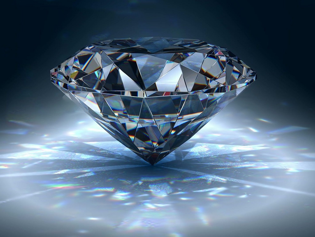
The diamond industry has undergone a remarkable transformation with the advent of CVD (Chemical Vapor Deposition) technology. Once known primarily for gemstones, diamonds are now recognized as one of the most advanced materials for industrial and scientific use. Among the many breakthroughs made possible by this innovation, CVD Single Crystal Diamond Wafers stand out as a true marvel combining the unmatched physical, thermal, and optical properties of natural diamond with the precision and scalability of modern manufacturing.
Today, these wafers are driving advancements in electronics, optics, quantum technology, and high-performance engineering, making them an essential component in the next generation of devices and systems.
What Are CVD Single Crystal Diamond Wafers?
CVD Single Crystal Diamond Wafers are ultra-pure diamond substrates created using the Chemical Vapor Deposition process, which allows carbon atoms to bond layer by layer under controlled conditions. Unlike natural diamonds, which form deep within the Earth over millions of years, CVD technology replicates the same process in a laboratory using advanced plasma systems delivering diamonds of extraordinary purity, uniformity, and consistency.
What makes single crystal diamond wafers unique is their crystalline perfection. Each wafer is made from a continuous, defect-free crystal lattice, ensuring superior optical clarity, electrical insulation, and thermal performance. These wafers can be precisely engineered to meet specific thickness, size, and orientation requirements, making them ideal for scientific research and high-tech applications.
How Are CVD Single Crystal Diamond Wafers Made?
The production of CVD single crystal diamond wafers involves a delicate balance of chemistry, physics, and precision engineering. The process typically follows these steps:
- Preparation of the Diamond Substrate
- A small seed of natural or synthetic single-crystal diamond is carefully cleaned and placed in a deposition chamber.
- The quality of this seed determines the orientation and growth of the resulting crystal.
- Gas Mixture Introduction
- A controlled mix of gases, primarily methane (CH₄) and hydrogen (H₂), is introduced into the chamber.
- Hydrogen acts as a stabilizer, preventing graphite formation and promoting diamond bonding.
- Plasma Activation
- The chamber is energized using microwave plasma (MPCVD), creating a high-energy environment where gas molecules break apart.
- Carbon atoms from methane separate and settle onto the diamond substrate.
- Crystal Growth
- Carbon atoms attach to the diamond seed in an ordered pattern, extending the crystal lattice layer by layer.
- This process continues for hours or days, depending on the desired thickness (often 0.5 mm to several millimeters).
- Cooling and Polishing
- After growth, the diamond wafer is slowly cooled to prevent stress fractures, then precisely cut, lapped, and polished to achieve optical-grade smoothness.
This meticulous process results in a flawless single crystal diamond wafer with exceptional material properties unmatched by any other substance.
Key Properties of CVD Single Crystal Diamond Wafers
CVD single crystal diamonds exhibit a combination of properties that make them ideal for high-performance industrial and scientific use:
- Exceptional Thermal Conductivity: Up to 2200 W/m·K, far surpassing copper, making it the best natural heat spreader.
- High Hardness and Wear Resistance: With a Mohs hardness of 10, diamond is the hardest known material.
- Electrical Insulation: Naturally non-conductive, ensuring safety and stability in electronic and power applications.
- High Optical Transparency: Excellent transmission across ultraviolet, visible, and infrared spectra.
- Low Coefficient of Thermal Expansion: Maintains dimensional stability under temperature fluctuations.
- Chemical Inertness: Resistant to acids, alkalis, and oxidation, even under extreme conditions.
These properties enable CVD diamond wafers to outperform conventional materials such as silicon, sapphire, or gallium nitride in demanding environments.
Applications of CVD Single Crystal Diamond Wafers
The versatility and reliability of CVD single crystal diamond wafers make them a preferred material across multiple industries.
- Electronics and Semiconductors
Diamond wafers are increasingly being used as heat spreaders and substrates for high-power electronic devices, including GaN (Gallium Nitride) and SiC (Silicon Carbide) components.
- They efficiently dissipate heat, preventing thermal damage and improving device longevity.
- Ideal for high-frequency transistors, power amplifiers, and radio frequency devices.
- Optics and Photonics
In optical engineering, CVD single crystal diamond wafers serve as:
- Optical windows, lenses, and mirrors for high-power lasers.
- Infrared windows in defense, aerospace, and spectroscopy applications.
- UV-transparent components in semiconductor lithography tools.
Their optical clarity and durability make them suitable for environments that require both precision and resilience.
- Quantum Technology
Diamonds containing nitrogen-vacancy (NV) centers, created through controlled doping during CVD growth, are a cornerstone of quantum computing and quantum sensing.
- They enable ultra-sensitive magnetic and temperature detection.
- Provide stability and coherence necessary for next-generation quantum processors.
- High-Performance Thermal Management
Due to their unmatched thermal conductivity, CVD diamond wafers are used as thermal spreaders and heat sinks in lasers, LEDs, and power electronics.
- They maintain optimal temperature levels even under extreme energy densities.
- Advanced Research and Industrial Tools
In scientific and industrial research, diamond wafers are used in X-ray windows, pressure anvils, and microwave components. Their ability to withstand high temperatures and pressures without degradation makes them indispensable in demanding environments.
Advantages of CVD Single Crystal Diamond Wafers
- Ultra-High Purity – Near-zero impurity levels ensure consistent optical and electrical performance.
- Scalability – CVD technology allows precise control over wafer size and thickness.
- Customization – Tailored properties for specific optical or electronic requirements.
- Eco-Friendly Production – Unlike mined diamonds, CVD growth is sustainable and ethical.
- Superior Reliability – Long-term performance stability under mechanical, thermal, and chemical stress.
CVD Single Crystal Diamond vs. Other Materials
|
Property |
Diamond |
Silicon |
Sapphire |
GaN |
|
Thermal Conductivity (W/m·K) |
2200 |
150 |
35 |
130 |
|
Hardness (Mohs) |
10 |
7 |
9 |
9 |
|
Optical Transparency |
UV–IR |
Limited |
UV–IR |
Visible–IR |
|
Electrical Conductivity |
Insulator |
Semiconductor |
Insulator |
Semiconductor |
|
Thermal Expansion (ppm/K) |
1.0 |
2.6 |
5.0 |
3.2 |
From this comparison, CVD single crystal diamond wafers clearly demonstrate superior performance across almost every critical parameter, making them an ideal choice for advanced engineering and scientific applications.
The Future of CVD Single Crystal Diamond Technology
As the world moves toward more compact, powerful, and energy-efficient systems, CVD single crystal diamond wafers are poised to play an even greater role in next-generation technology. Researchers are exploring:
- Larger wafer sizes (over 6 inches) for semiconductor integration.
- Doped diamond structures for electronic and quantum applications.
- Hybrid materials combining diamond with silicon or GaN for advanced circuit design.
- Automation and AI-based growth control for faster, defect-free production.
With these advancements, diamond is rapidly transitioning from a luxury gemstone to a critical engineering material powering the future of electronics, optics, and energy systems.
Conclusion
CVD Single Crystal Diamond Wafers represent the pinnacle of precision materials engineering combining the natural brilliance of diamond with the control and repeatability of modern technology. Their exceptional thermal, optical, and mechanical properties make them indispensable in cutting-edge fields such as electronics, photonics, and quantum science.
As industries demand higher performance and sustainability, CVD diamond wafers are set to redefine what’s possible in advanced material applications. They are not just the future of the diamond industry they are the future of innovation itself.


